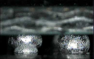
Several years ago Intel Corporation highlighted a defect that was aptly named Non-Wet Open (NWO). Others have referred to it as “hanging ball”. It is a soldering defect associated with bumped components, specifically bumped components that are made of very thin organic substrates, such as Intel’s Haswell and Ivy Bridge processors. This defect was recently written about by my colleague, Derrick Herron here.
NWO is very simple in its nature. Solder paste is stencil-printed onto, typically, a thin FR4 printed circuit board. The bumped component is placed, along with other SMT devices, and the assembly is sent through a reflow oven to effect the soldering of the SMT components to the PCB. Because of the thin nature of the substrates used in the construction of the bumped component, along with, often, multiple silicon die nonsymmetrically located on the surface of the organic substrate, the bumped component has some amount of warpage from the get-go. Furthermore, again owing to the thin nature of the bumped component substrate with multiple nonsymmetrically located silicon die and often very thin printed circuit boards, a considerable amount of warpage of both the bumped component and printed circuit board occurs during the reflow cycle. As the corners and edges of the bumped component warp away from the surface of the PCB, the solder paste deposits adhere to the peripheral bumps and get lifted off of the pads. During this separation, the solder paste reflows and combines with the solder bump on the component. The solder paste never successfully wets to the pad and NWOs are created.
This phenomenon is most prevalent with OSP-coated copper pads. It can occur with other pad finishes like ENIG, Immersion Sn, and Immersion Ag, but seldom does. This is because the OSP coating on the pad is organic and non-metallic. The solder paste preferentially adheres and wets to a metallic surface like the solder bump on the component as opposed to this organic coating.
Solder pastes that are designed to mitigate NWOs have a flux chemistry which eats through the OSP coating, allowing the tin in the solder alloy particles to diffuse into the copper and to start bonding to it so that it stays stuck to the pad and does not lift off when the component warps. It is possible that this may end up creating another defect called HIP (Head in Pillow) where the solder paste deposited on the PCB pad stays stuck to the pad and the bump separates from it as the component warps upward and away. But, this can generally be remedied rather easily by enlarging the aperture size to create a bigger paste deposit.


