Related Semiconductor Flux Technical Documents
Application Notes
- Storage and Handling of Specialty Fluxes (US Letter)
Flux is a compound that, when heated, helps remove oxides off solderable surfaces, which is critical in allowing them to bond to each other. As almost every metal and alloy will grow an oxide layer over time, flux is one of the most important materials if you are soldering by-hand or in a reflow oven. Because of this, many people want to know: what type of flux should we be using? Read more to find out!
Read MoreSIR Testing-Surface and Insulation Resistance testing, a form of standard testing where you measure the electrical reliability of a no-clean or a water-soluble flux residue, has existed for a while now.
Read MoreViscosity and tack are two important material properties that define a flux. People often “tack” them together as one, thinking they go hand-in-hand. Typically, this is the case, but not always. This blog discusses the differences between these properties.
Read MoreJim Hisert enlists Meagan Sloan, Technical Support Engineer to recommend a flux for his indium preform application.
Read MoreThe different flux and solder paste formulations mean that some products will have different material lifetimes than others. Understanding the lifetimes and following manufacturers recommendations can help to ensure you get the optimum performance from the material.
Read More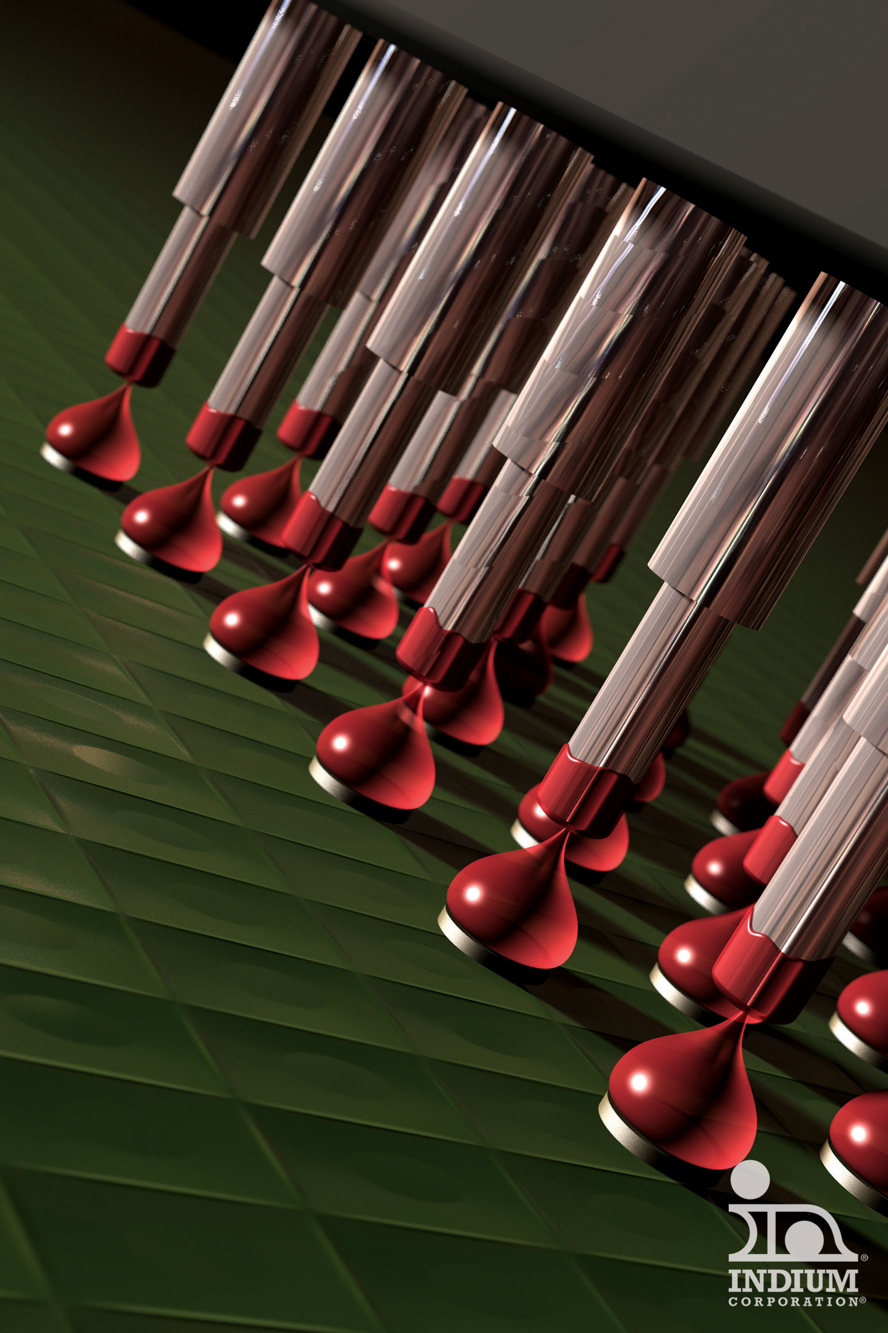
The ball-attach process for BGA and PGA packages uses a flux that is usually applied via pin-transfer from a dipping tray. Solder spheres (solder balls) are then placed into the deposits and the whole assembly is reflowed. BGA fluxes are usually water soluble, while PGA fluxes are often very reactive no-clean materials.
Indium Corporation most popular ball-attach fluxes include:
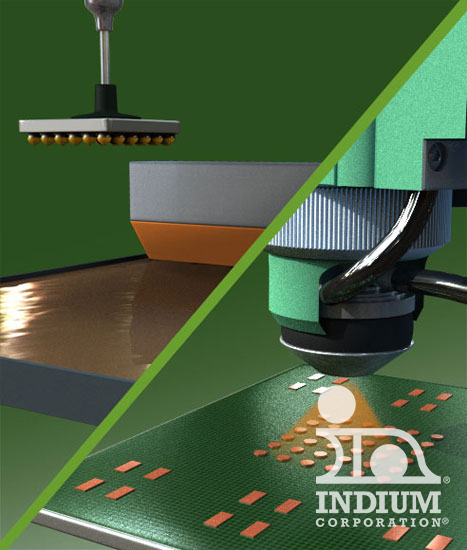
The flip-chip process involves taking the singulated die from a wafer mounted on a wafer dicing tape, inverting ("flipping") them and placing them onto a substrate. The substrate may be a printed circuit board, a ceramic substrate, or (in the case of 2.5D and 3D assembly) an interposer.
Copper pillar/solder microbumps are emerging as a standard flip-chip solder bump replacement in many parts of the semiconductor assembly industry, from standard chip-attach to power devices using flip-chip on leadframe as assembly technologies. For logic and similar devices, substrate metallization (landing pad) technology has also shifted from solder-on-pad (SoP), manufactured from printed and reflowed and cleaned solder paste, to individual solder balls. The technology is now moving to simple organic solderability preservative (OSP) on copper.
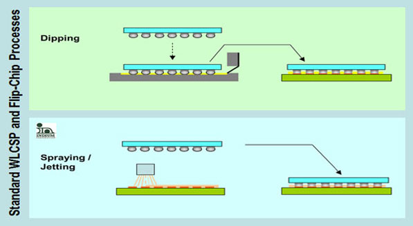
Water-soluble fluxes, which may be applied by dipping or spraying, have long been used in flip-chip assembly, but their long history of utility is facing multiple challenges as a number of factors makes the move to no-clean inevitable in the high-volume sub-130micron copper pillar era.
The use of copper pillar instead of solder bumps has meant that chip-substrate clearances and finer pitches do not necessarily move in lock-step with each other. However, copper pillar heights of 40-60 microns (and even shorter than this in the near future) combined with fine pitch, makes cleaning extremely complex. Aqueous (water-based) cleaning becomes more complex with fine pitch flip-chip attach as it becomes increasingly difficult to get the cleaning solution under the chip to dissolve the residues, and then to carry the residue-containing solution out from under the chip.
A recent emerging failure mode caused by cleaning involves solder joint damage during aqueous jet impingement. This failure mode is believed to be driven by a combination of: very small diameter microbumps; the move from hemispherical to very thin solder microbumps on copper pillar (reduced joint compliance); and low CTE, low-cost, and low layer count (thinned) substrates. In these circumstances, a move towards an ultra-low residue no-clean flux is inevitable, although new failure modes continue to appear, being driven by the smaller dimensions. For this reason, Indium Corporation has introduced a series of ultra-low residue (ULR) fluxes called NC-699, NC-26-A, and NC-26S for both current and emerging applications.
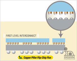
Cu-Pillar Flip-Chip Flux is a dipping flux designed for use in thermocompression bonding flip-chip copper pillar applications. Its rheology and chemical design enables its use with dipping depths down to 10 microns or less.
The amount of flux deposited on the substrate can be optimized by changing equipment parameters. Key variables include temperature, copper-pillar dimensions, shear speed, time of shearing before dipping, dwell time in flux, and depth of immersion. The flux rheology can be optimized for the desired application by shearing to achieve the desired viscosity.
Packaging is available in 10cc and 30cc syringes.
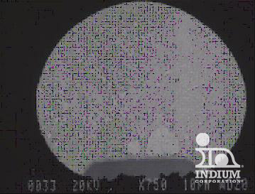
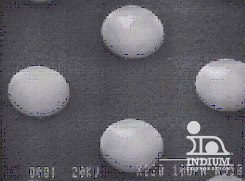
Wafer bumping flux, which is also referred to as bump fusion flux, is a low-viscosity flux spin coated onto solder-bumped and copper-pillar or solder-capped wafers. The flux is designed to remove oxide and other contamination during reflow and cleaning steps. It converts rough, non-spherical, plated or wafer probe-dented solder bumps into shiny, oxide-free bumps. These fluxes can be either water-soluble or solvent clean.
Standard products include (chart):
| Flux Type | Flux Application Method | Description | Cleaning Method | Halogen-Free | Material |
|---|---|---|---|---|---|
| SC | Dispense/Spin Coating | High Pb, SnPb eutectic, and SnAg solder bumps | Solvent or aqueous-based chemistry | YES | SC-5R |
| WS | Dispense/Spin Coating | 20-65 micron pitch copper-pillars with SnAg or Sn100 microbumps | Warm DI water | YES | WS-3401 WS-3543 |
| Considerations | Solder Paste Printing |
Plating | Flux/Solder Ball Printing |
C4-NP (Suess/IBM) |
|---|---|---|---|---|
| Used In High Volume Manufacturing? | Yes | Yes | Yes | Yes |
| Alloy Restrictions | All solder alloys, as long as powder can be made | Binary alloys only (Sn/Pb, Sn/Ag, Sn/Cu etc.) due to alloy control issues | All solder alloys, as long as sphere can be made | Probably limited to binary alloys |
| Bump Size | Down to around 125micron pitch only. Only 45% of paste volume is metal | Down to 2micron bumps feasible: possibly less | 60micron bump diameter in mass production, but most commonly used for wafer level CSP manufacturing | Unknown |
| Bump Uniformity | OK: can vary significantly with age of solder paste and print process variables | Good | Good with appropriate tight tolerance solderspheres | Good |
| Voiding | Common | Little or no with a controlled plating process | Little or no | Little or no |
| Cost Comparison | Low Cost | More Expensive | Low Cost | High Capital Cost |
| Prototyping | Fairly Easy | Complex | Easy | Complex |