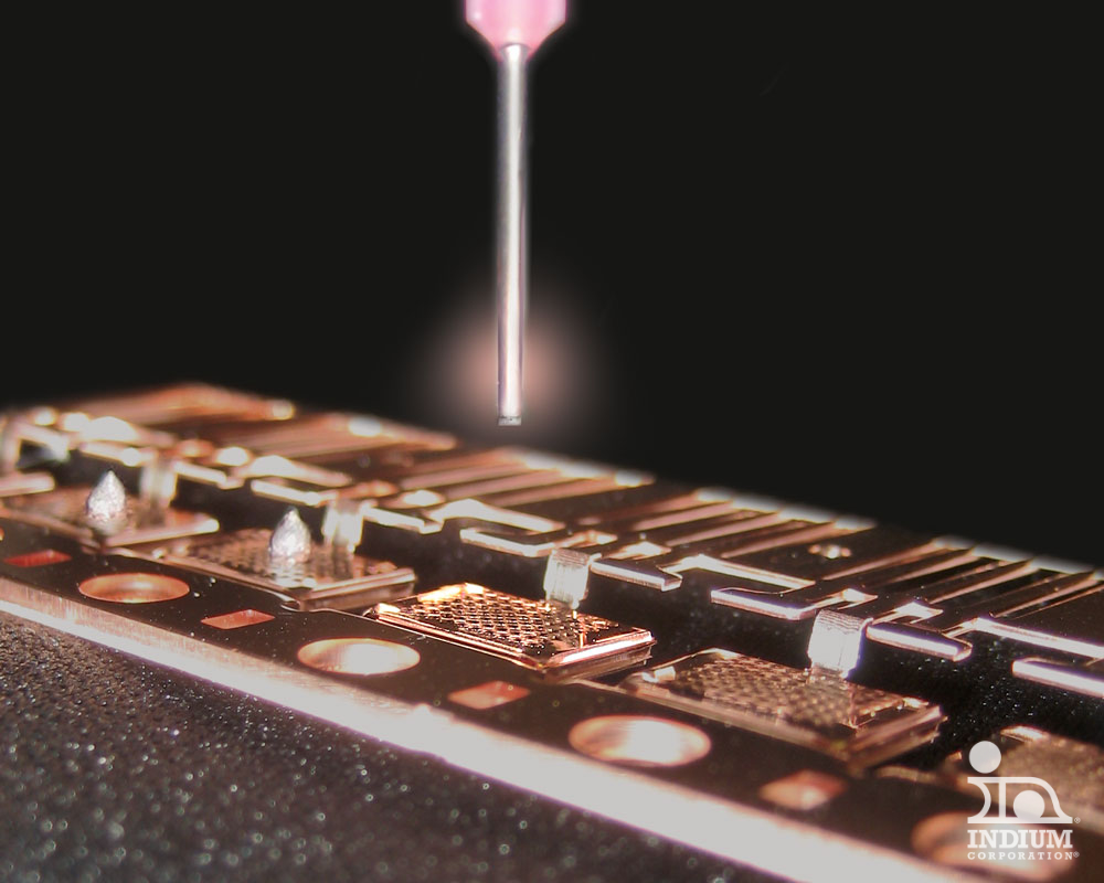
Related Semiconductor and Advanced Assembly Videos
Related Semiconductor and Advanced Assembly Blog Articles
Interconnect Reliability: From the Chip to the System
Interconnect reliability is critical to the reliability of semiconductor packaging and electronic systems. If we look at the life cycle from the chip to the system—from IC design, wafer fab, and packaging, to board assembly and system integration—the common element is the “interconnect thread” for the reliability of the electronic system in the field...
Read MoreTrade Show Travels June 2022
Where has the semiconductor team been traveling to this summer?
Read MoreSiP Printing 101 Webinar Preview: Stencil Technology
Stencil technology has evolved throughout the years, and System-in-Package solder pastes require specific stencil manufacturing processes and novel technology to achieve great transfer efficiency. Learn more at my upcoming SiP Printing 101 Webinar!
Read MoreSiP Printing 101 Webinar Preview: Solder Paste Inspection
Just as important in the solder paste printing process is solder paste inspection; how do you know if your printer is operating optimally if your SPI machine is not doing the same? Learn more in my upcoming SiP Printing 101 Webinar.
Read MoreSiP Printing 101 Webinar Preview: Water Soluble vs. No-Clean Pastes
Choosing the correct solder paste formulation is critical for System-in-Package assembly. Indium Corporation's SiPaste® solder pastes offer a complete portfolio of pastes to choose from to fit many assembly processes. Learn more in the upcoming SiP Printing 101 Webinar!
Read MoreIndium Corporation products are used in the manufacture of mobile devices, such as cell phones, tablet computers, computer games, automotive electronics, avionics, server farms, and power handling for renewable energy sources.
- 2.5D and 3D packages
- Ball-attach
- Die-attach
- Flip-chip
- SiP and heterogenous integration

2.5D and 3D Packaging
Indium Corporation is a world leader in the design, formulation, manufacture and supply of semiconductor-grade fluxes and associated materials, enabling 2.5 and 3D assembly processes, as well as more standard flip-chip assembly.
We continue to work with leading customers and equipment partners to develop and optimize materials and associated assembly processes in this rapidly expanding area of technology.
Our offerings include:
- Bump fusion (wafer) fluxes for copper pillar / microbump formation
- 2.5D/3D fluxes for thermocompression bonding (TCB) assembly:
- Memory-stacking (memory cube)
- Memory on logic (3D)
- Logic and memory on interposer (2.5D)
- Standard flip-chip fluxes
Ball-Attach
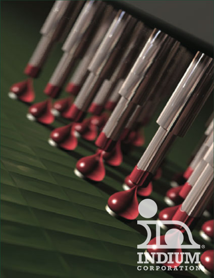
The ball-attach process for BGA and PGA packages uses a flux that is usually applied via pin-transfer from a dipping tray. Solder spheres (solder balls) are then placed into the deposits and the whole assembly is reflowed. BGA fluxes are usually water soluble, while PGA fluxes are often very reactive no-clean materials.
Our Applications
WS-446HF
A no-intentionally-added halogen-free water washable ball-attach flux with an activator system powerful enough to promote wetting on the most demanding substrate metallizations
WS-575-C-RT
A halogen-compliant, room temperature stable, one-step flux that eliminates the need for pre-fluxing
WS-3600
A robust, halogen-containing flux that works well under challenging conditions
NC-585
Designed for PGA applications; eliminates issues caused by cleaning while still ensuring good solderability

Bump Fusion
Indium Corporation’s wafer bumping (bump fusion) fluxes are low-viscosity fluxes spun onto solder-bumped and copper-pillar/solder-capped wafers. They are designed to remove oxides and other contamination during the reflow and cleaning steps. These fluxes are halogen-free and can be applied via dispense or spin coating.
Flip-Chip
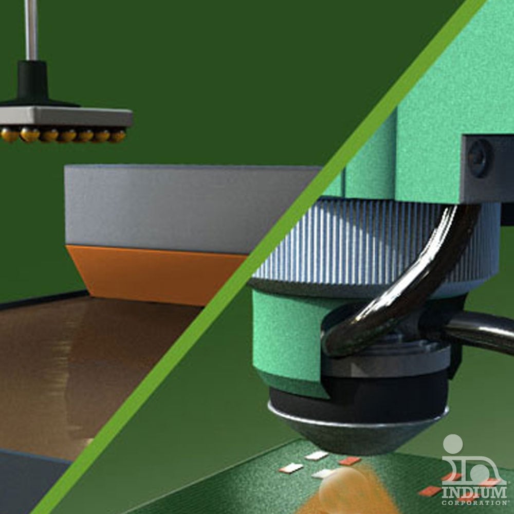
The flip-chip process involves taking the singulated die from a wafer mounted on a wafer dicing tape, inverting ("flipping") them and placing them onto a substrate. The substrate may be a printed circuit board, a ceramic substrate, or (in the case of 2.5D and 3D assembly) an interposer.
Copper pillar/solder microbumps are emerging as a standard flip-chip solder bump replacement in many parts of the semiconductor assembly industry, from standard chip-attach to power devices using flip-chip on leadframe as assembly technologies. For logic and similar devices, substrate metallization (landing pad) technology has also shifted from solder-on-pad (SoP), manufactured from printed and reflowed and cleaned solder paste, to individual solder balls. The technology is now moving to simple organic solderability protectant (OSP) on copper.

SiP & Heterogeneous Integration & Assembly (HIA)
From water-soluble to no-clean soldering solutions, Indium Corporation’s portfolio of products meets current and evolving challenges encountered in fine-pitch HIA and SiP applications.
Indium Corporation’s soldering materials for Heterogeneous Integration & Assembly (HIA) and system-in-package (SiP) applications have a PROVEN track record with more than 2 billion SiP front-end module (FEM) SiP devices manufactured in the last 3 years using Indium Corporation materials.

