Folks,
The advent of 0201 and even 01005 passives and CSPs with 30 mil lead spacings necessitate very small solder deposits in the stencil printing process. These solder deposits can be so small, that when reflowed, they can result in a single solder grain. Typically a single solder grain will have poor mechanical properties, however this is especially the case when the C axis of the solder grain is parallel to the PWB pad (i.e. parallel to the direction of maximum stress).
To minimize this concern, you should make sure that the cooing rate on your reflow oven is higher than 2 degrees C/sec. Solder metallurgists are also studying this phenomenon to minimizeits impact.Currently"dopant" levelsof titanium, which suppresses undercooling and nickel or cobalt which refines grain size are being investigated. As miniaturization continues, it wouldn't be surprising if some solder pastes are designed to minimize this single solder grain concern.
Cheers,
Dr. Ron
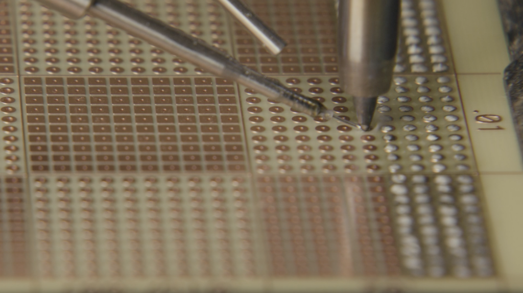
Note: The photo of passives is from a paper I co-authored, Process Development for 01005 Lead-Free Passive Assembly:
Stencil Printing, Joe belmonte etal at APEX 2007, Los Angeles.
.


