Folks,
This post is an excerpt on graping, fromIndium Corporation'sThe Printed Circuits Assemblers Guide to Solder Defects.
Introduction
The growth of personal electronic devices continues to drive the need for ever-smaller active and passive electrical components. This miniaturization trend, together with the demands for RoHS-compliant Pb-free assembly, has created more challenges, including the graping effect.
As a solder paste deposit decreases in size, the relative surface area of exposed solder particles increases, and the amount of available flux to remove surface oxides decreases. Compounding this is the additional heat necessary to reflow most Pb-free solders, resulting in a formula conducive to producing the graping phenomenon. During the heating process, as the flux viscosity decreases and begins to spread downward and outward, the solder particles are exposed at the top of the solder paste deposit. If there is no flux in proximity, these solder particles may become oxidized when the solder paste enters the ramp or soak stage of reflow. These oxides will inhibit the full coalescence of the particles into a uniform solder joint when the solder is liquidus. The unreflowed particles often exhibit the appearance of a cluster of grapes, as can be seen in Figure 1.
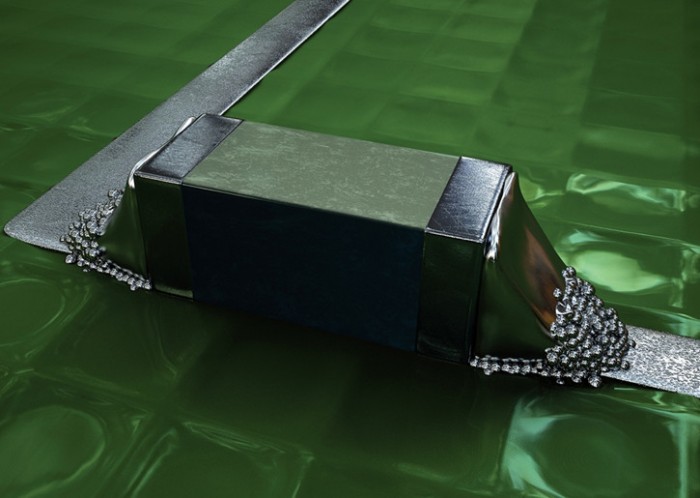
Figure 1. The graping effect.
Stencil Printing
The area ratio (AR) is a critical metric in successful stencil printing. It is defined as the area of the stencil aperture opening divided by the area of the aperture sidewalls. Figure 2 shows a schematic for square/rectangular and circular apertures. A simple calculation shows that the AR is simplified to the diameter (D) of the circle divided by four times the stencil thickness (t) or AR=D/4t. Somewhat surprisingly, the result is the same for square apertures, with D now equal to the sides of the square. For the AR of a rectangular aperture, the formula is a little more complicated: ab/2(a+b)t, where a and b are the sides of the rectangle.
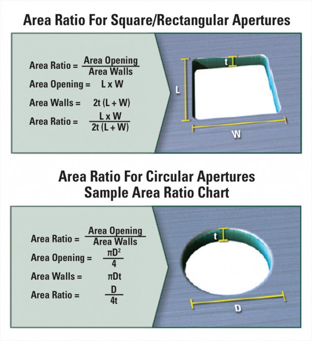
Figure 2.Aperture schematics for rectangular and circular apertures.
It is widely accepted in the industry that in order to get good stencil printing, the AR must be greater than 0.66. Experience has shown that if the AR <0.66, the transfer efficiency could be low and erratic, although this has gotten better with advances in solder paste technology.
Transfer Efficiency
Transfer efficiency, another important stencil printing metric, is defined as the volume of the solder paste deposit divided by the volume of the aperture. To accommodate fine-feature stencil printing, it is not uncommon to look at solder paste that incorporates finer powder in order to optimize the printing process. However, as the size of the powder particles within the solder paste decreases, the relative amount of surface area exposed increases. With this increase in surface area, an increase in total surface oxides is also introduced. This increase in surface oxides requires the flux chemicals to work even harder at removing the oxides and protecting the surfaces of the powder, component, and board metallizations during the entire reflow process.
On a 3mil-thick stencil, the AR for a 6mil square aperture is the same as the AR for a 6mil circular aperture: 0.50. However, when comparing the two, the volume of the square solder paste deposit is greater (~108 cubic mil) than the circular deposit (85 cubic mil). The additional solder paste volume provided by the square aperture may help reduce graping. Of greater importance, though, is the increased transfer efficiency provided by the square aperture. The square aperture design provides more consistent transfer efficiency, further reducing the potential for graping as inconsistent deposits could mean less volume.
SMD vs. NSMD Pads
Results from solder masking experiments have shown that the graping effect is less prevalent for the solder mask defined (SMD) pads. It is believed that the solder mask provides a barrier (dam), restricting the spread of the flux during the heating process, and increases the potential availability of the flux to remove oxides and protect from further oxidation. The solder mask can also act as a barrier to protect the solder paste powder particles in close proximity from further oxidation.
Water-Soluble vs. No-Clean
No-clean flux chemistries are generally rosin/resin-based (hereafter referred to only as resin) formulas. Because resins are not very soluble in the solvents used in water-soluble flux chemistries, they are typically replaced with large molecular compounds, such as polymers, in water-soluble fluxes. The activator(s) within the flux chemistry removes the current oxides on the joining surfaces, as well as the solder paste powder particles within the solder paste itself. Further oxidation/re-oxidation does occur during the heating stage. Whereas the resins in no-clean fluxes are excellent oxidation barriers and protect against re-oxidation, the lack of resins in water-soluble chemistries cause them to fall short in terms of providing oxidation resistance.
Hence, for the same reflow profiles—though water-soluble chemistries are generally more active—the lower oxidation resistance of water-soluble chemistries makes them more sensitive in long and/or hot profiles, increasing the potential for graping defects.
Ramp-To-Peak vs. Soak
For many years, the “soak type” reflow profile was quite prevalent. Over time, however, focus has shifted to ramp-to-peak (RTP) as the preferred reflow profile. Contributing to this shift is the higher reflow process temperatures associated with Pb-free solders, as well as the need to diminish the total heat exposure of the smaller paste deposits and temperature-sensitive components and board laminate. Another benefit of the soak profile is its utilization to reduce voiding. However, it is not as effective with Pb-free solders, due to the increased surface tension of Pb-free solders and the higher temperature used to reflow them.
To minimize graping, a reduced oven time is better, provided you use the same time-above-liquidus (TAL) and peak temperature, see Figure 3. The soak profile typically produces more graping than an RTP profile. The graping effect is exacerbated as the total time in the oven increases. Decreasing the total heat dramatically decreases the graping effect. A ramp rate (from ambient to peak) of 1°C/second is commonly recommended, which equates to approximately 3 minutes, 40 seconds to a peak temperature of 245°C.
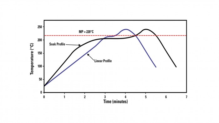
Figure 3.Typical reflow Pb-free profiles.
Conclusions
To reduce the graping effect, it is vital to ensure an optimal printing and reflow process. Using the guidelines provided for the area ratio and good process/equipment setup will ensure good transfer efficiency. Though the area ratio for circular and square aperture designs may be equal, the potential for graping increases with circular aperture designs due to decreased paste volume and decreased transfer efficiency.
From a reflow standpoint, decreasing the total heat input will decrease the likelihood of the effect. Using an RTP-type profile with a ramp rate of ~1°C/second is suggested.
Material factors also influence the outcome. The observance of graping increases as the solder paste particle size decreases and the area of surface oxides increases. Water-soluble solder paste chemistries do not provide the oxidation barrier that resins do for no-clean chemistries and are more prone to the graping effect.
Cheers,
Dr. Ron

