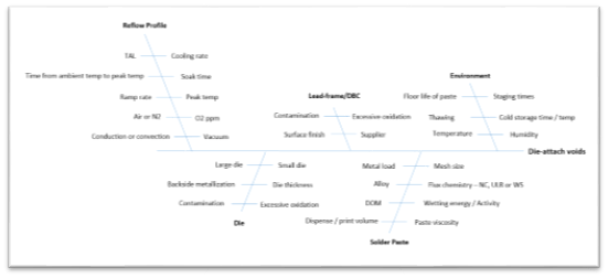
“How do I reduce my die-attach soldering voids?” is a question I am often asked by customers in the power semiconductor field. Excessive voids are bad news in die-attach applications, not only because they affect the joint mechanically as a place where cracks can propagate, but also because they affect the electrical and thermal conductivity of the device. How great it would be if there was a simple answer, a silver bullet if you will, for solving this problem. But, the fact of the matter is every case is different.
That being said, the various factors that affect voiding will, by and large, be common, and identifying the potential factors that contribute to voiding can be essential in determining the root cause.
One statistical tool that can be used to visually map out the potential factors is the Ishikawa, or fish bone, diagram. It is also known as a cause-and-effect diagram, the potential causes make up the “bones” which can all lead to the effect seen at the “head” of the horizontal axis.

Having the potential causes mapped out in such a way helps when deciding where to focus your efforts to reduce die-attach soldering voids. To mitigate the environmental causes, be sure to follow the storage and handling recommendations of your solder paste supplier. It goes without saying that good practices in handling the die and lead-frame/DBC to minimize contamination will go a long way in the battle against voiding. That brings us to the two remaining categories which have the most potential causes for die-attach voids: the reflow profile and the solder paste.
- The reflow profile can have a significant effect on die-attach voids as every aspect of the reflow process can have an impact. The peak temperature needs to be suitably high enough to melt the alloy you are using, form a good metallurgical bond, and lower the surface tension of the molten solder enough to allow the flux volatiles outgassing (potential voids) to escape, but not be too high and potentially cause flux charring and de-wetting. The time it takes to go from ambient to peak temperature, the ramp rate, and soaking time (if present) can all affect the rate at which flux volatiles activate and outgas. The TAL, or time-above-liquidus, needs to be long enough for flux volatiles outgassing to escape (especially under larger die), but too long and it can result in excessive outgassing that cannot escape. Finally, there is the reflow atmosphere. For die-attach reflow it is “the norm” to reflow under nitrogen or forming gas as the void requirements of most customers cannot be consistently achieved under air. A ppm of 02 may need to be controlled below a certain level for certain solder pastes to work effectively. For higher power devices such as IGBTs, where the requirements for voiding are even stricter, it is now very common to use a vacuum reflow system.
- The last, and arguably most important factor we will look at is the solder paste itself. Using the optimal combination of alloy, flux chemistry, metal load (% of metal in the paste by weight), and powder type (mesh size) for your specific application and process is the best weapon in the combat against die-attach voiding.
All of Indium Corporation’s technical support engineers (myself included) are on hand to help you with your solder paste selection and process optimization to enable you Avoid The Void™.
If you have any questions, be sure to reach out to any one of us.


