You may remember that, a couple of years ago, I wrote an article for Chip Scale Review magazine about plans for a major semiconductor facility (the Marcy Nanocenter). Well, sometimes wishes DO come true! The recent announcement of the CNSE (College of Nanoscale Science and Technology at Albany NY) as end user for semiconductor-ready buildings to be constructed in coming years is generating a lot of interest. Cynics will say, "Why is that, as it looks at first glance to be one hand washing another at public expense?"
Those of you who have been keeping tabs on developments may remember that, at the end of 2012, the Army Corps of Engineers turned down a wetlands construction permit due to the absence of such an end user. If you can’t get a permit without an end-user… and it is claimed that Marcy can not get end users without the permit, you end up in a catch 22. So, in reality, CNSE is merely breaking the vicious cycle.
The numbers (and CNSE can be forgiven little hyperbole here) are for three 450mm fabs at $10-15BN and 450,000square feet each in Marcy. The project will be funded by a mix of public and private investment. But, what will actually be made here, and by whom? Intel has already said it is not interested in the Marcy site, leaving Samsung and TSMC as the others of the triumvirate of potential candidates likely to want to build a wafer fab there. An actual fab, therefore, seems rather unlikely. So, what could be the future for the location? Please let me indulge a little speculation (the below IS only conjecture) and we’ll see where that takes us:
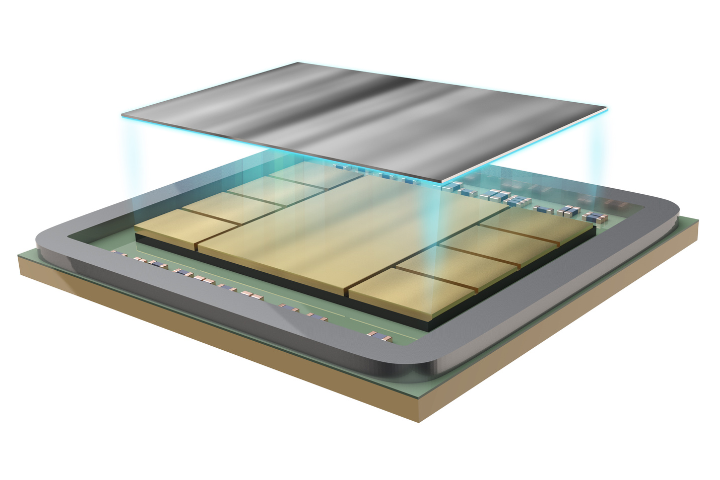
Semiconductor Assembly: As always, this is very dear to my heart! With Global Foundries just down the road (OK: 90miles, but still pretty close), Marcy could expand into post-BEOL processing for GloFo, including 2.5D and 3D assembly and wafer-on-wafer (although John Lau said last year at IWLPC that he thought wafer-on-wafer would be “2020… maybe”). If you’re doing 3D, that would also involve a major memory company for the memory cube: and how those are made and transported may be a key factor in feasibility. I haven’t actually seen the HMC yet, and the unusual stacked device in the background in the photo within the recent Micron announcement is probably just a marketing diagram.
OSAT: It is possible that Amkor, ASE, StatsChipPAC , SPIL, or PTI may want to build 2.5D packaging / post-BEOL processing facilities. The increasingly vertical integration of some of the wafer fabs also doesn’t take that possibility off the table either.
Power Wafer Fabrication: After Infineon announced its 300mm GaN-on-silicon manufacturing, it is just in the realm of possibility that a larger III/V (GaN/GaAs/InP) or even II/IV (SiC) wafer facility could be built, possibly alongside a….
Power OSAT: As the usage of power electronics, especially in electric vehicles such as the Tesla, and for large Green power infrastructure, expands, this will mean an increasingneed for US capability in high voltage, high power IGBT andother power device module manufacture. A company like Infineon or Toshibacould do both the power wafer fab and the device packaging/assembly.
Silicon Photonics: Even more intriguing was a discussion at the 2013 MEPTEC Roadmapping meeting in San Jose that 3D stacking is merely a stopgap measure on the way to photonic integration. This may be a little more far-sighted, positioning the Marcy Nanocenter well for 2020 and the evolution of the "Internet of Things".
For the first two considerations, the devil in the details is how easily and, hence, how FAR thinned wafers and memory cubes can be transported without physical damage, and whether it makes any economic or logistical sense. The longer a wafer sits before it turns into a chip is just money sitting idle.
Infrastucture also poses some short term food for thought. Does Marcy have enough water of the appropriate purity to supply 3 fabs without excessive pretreatment? Is the power supply stable enough, even in the depths of a Lake Effect snow or ice storm? These are serious questions that need to be answered.
There’s a Chinese sayingabout “interesting times”, too. So, maybe let’s hope for “intriguing times” instead for the Marcy/Utica, NY area – it is certainly a beautiful place to live.
Cheers!
Andy


